BACK-END LIBRARIES
Libraries are the most critical parts of complete ASIC design because the measure of accuracy of these libraries has great impact on both success and failure of ASIC design. Three types of cells to be placed in physical design stage are
1) standard cells
2) macro cells
3) I/O pads
Among these Standard cell library and I/O pad library are typically used in ASIC physical design. The second cell to be placed will be in the form of GDS (Graphical Data Stream) or hard IPs. The macro cell’s all violations regarding timing and physical are already fixed and there is no need to touch the internal part of the cell.Macros are the outcome of block level designs.
STANDARD CELL PHYSICAL DESIGN
Standard cell is a specific design for each gate. Special care need to be taken during the process of physical design of such libraries in-order to achieve optimum die size and performance. Optimum area can be achieved by minimizing the routing area rather than minimizing the number of transistors. This is because of ASIC’s complexity due to shrinking and scaling.
Routing within standard cells have to be minimized because of most of the ASIC’s routing is done automatically by tool itself. So optimized design can be achieved by making the standard cells routing as optimized. Main parameters to be considered in standard cell library designing is
1) spacing rules
2) height of the cell
3) I/O ports location
1) Spacing Rules
Basic step in spacing rules begins with horizontal and vertical wire track determination. Wire tracks are nothing but horizontal and vertical lines drawn on the layout area. Wire tracks acts like guidelines for making the interconnections. Spacing, width are fixed to avoid spacing related issues in the further stages. In three ways wire track spacing is done as mentioned below
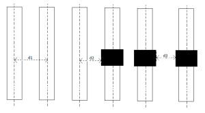
i) lint to line –> d1
ii) via to line (or) line to via –> d2
iii) via to via –> d3
The spacing is as mentioned below in figure-1.
Among the three ways, choosing the appropriate one and fixing it as common spacing throughout the library is the challenge. Choosing one appropriate spacing for the library will be effective only if the condition d3> d2> d1 is followed.
Fixing the via to via (d3) spacing distance for all designs in a library leads to more spacing and as a result of this routing will not be optimum. fixing line to line (d1) spacing distance for all designs in a library leads to less spacing between metals and logic and as a result of this routing will face DRC violations. Therefore fixing via to line (d2) for all design within a library satisfies both line to line and via to via spacing constraints. Routing will be optimum by using via to line (d2) for all conducting layer spacing rules and compact routing can be achieved. Since most of the ASIC’s routing is carried out automatically by software tool itself, optimized routing will be achieved by effective routing of interconnects of standard cell.
2) Height of the cell
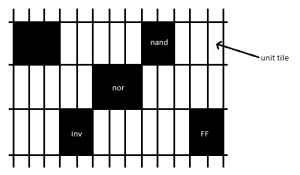
unit tile: It is a minimum height and width of the cell to be placed. These measures are available in the technology library. Unit tile is also known as site.
From the unit tile it is clear that the height of the standard cells to be placed should be the same, because these cells are to be placed on the placement rows in block-level or chip-level designs. Generally height of the standard cell is equal to the height of placement rows.. various width of the cell is available according to functionality and the drive strength of the cell and the width of the standard cell should be the multiple of width of the unit tile.
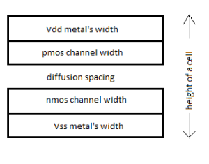
A Complementary Metal Oxide Semiconductor (CMOS) design has a height equal to the sum of Vdd’s width, pmos channel width, diffusion spacing between pull-up and pull-down transistors, nmos channel width and the width of Vss metal layer. Clear picture of this is shown below in figure-3.
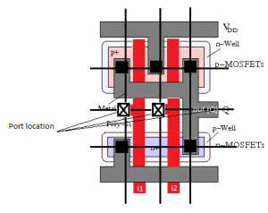
Once wire tracks and height of the cell are determined it is given to the standard cell layout in the form of wire track template. This wire track template is laid on the layout (fig-4) to ensure whether it meets all requirements of software tool or not. Width of the Vdd and Vss should be considerably stable in-order to provide proper current flow capability. Less width of Vdd and Vss will provide degraded 1 and 0 to power and ground respectively which in turn affects the overall performance of the design and relatively more width will affect the standard cell’s height. Width should be stable enough to provide strong 1 and 0 to vdd and vss respectively. High resistance in Vdd and Vss metal leads to latch-up phenomena.
Today’s EDA tool provide high flexibility in choosing the metal layer such as first metal traverse in vertical direction and second metal traverse in horizontal direction. This is an added advantage in standard cell physical design. Internal node capacitance need to be kept minimum, especially with nodes close to Vdd and Vss in-order avoid body effect.
3) Fixing I/O Pin or Ports
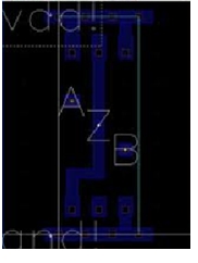
Another factor in standard cell physical design need to be taken care is fixing the physical location of I/O ports. It is advisable to use M1 for routing between the transistors.Placing the ports where exactly horizontal and vertical wire tracks cross each other yields better results because of reduce in routing complexity. This is called Port accessibility. This improves execution time during routing and produces better quality results. Pictorial representation of port accessibility is shown below in figure-4.
If routing is done with the help of wire track lines geometrical regularities withing same type of cells will be the same. Maintaining the geometrical regularities among the standard cells of same type has two main advantages.
– allows size reduction to another process node or another set of DRC rules
– common electrical characteristics helps in deciding the pmos and nmos channel width within the library.
Placing nmos transistors near Vss and placing pmos transistors near Vdd will also reduce the routing resources considerably because of CMOS design’s nature.
The final outcome of standard cell physical design is available in the form of lef(Layout Exchange Format). It is a very popular format for abstract view of library. Otherwise called as physical library.
